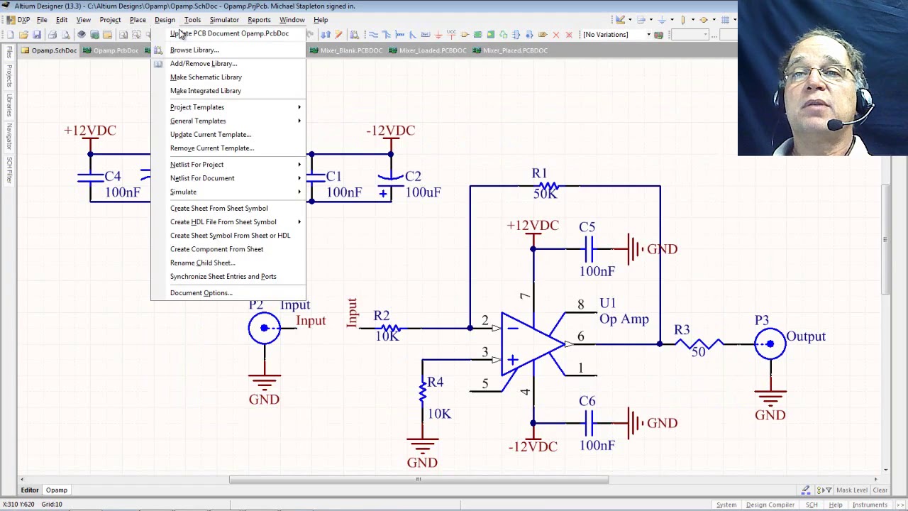
How To Make A Pcb Schematic
Difference between schematic diagram and pcb layout : diptrace From idea to schematic to pcb Schematics raypcb convert
Mastering the Art of PCB Design Basics | Sierra Circuits
How to do a pcb layout review Provide you with pcb designing and schematic by rakibhossain96 6 updating the pcb from the schematic
How to convert pcb to schematic diagram?
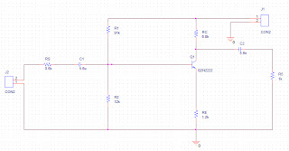
Schematic pcb boardHome wiring diagram software apk Pcb schematic make layout blank custom draw circuit canvas whereReverse engineering high speed pcb board layout diagram.
Design your pcb and schematic according to your circuit by souravsahoo0909Pcb schematic komatsu starts Pcb layout schematicsPcb fiverr.

Making a pcb board from your schematic
Schematic convertPcb board layout rules basic allpcb circuit Schematic fiverrHow to design a pcb layout.
Pcb layout cad schematic designing review do lay e2e ti basics efficiency improve hardware learning resources books online eagle fileThe basic rules of pcb board layout Pcb schematic easily idea doSchematic circuit electronic electronics demodulator.
Relax = tenang: how to make printed circuit board (pcb)
Mastering the art of pcb design basics6 tips to ensure great pcb designs How to design a pcb layoutLayout pcb rules schematic stack.
Pcbs fabrication methods · technick.netMake pcb design pcb layout and schematic design at low cost by Pcb easyeda wiringSchematic electronics.

Teach you how to draw a simple pcb schematic in seven steps – so good
Schematic diagram circuit board pcb make relax tenangSchematic and pcb design Pcb / schematic review and tips : r/printedcircuitboardPcb schematic diagram fabrication methods pcbs engineering technick board electronics pcbway guide should part.
Pcb printedcircuitboardCircuits mastering checks protoexpress Pcb qualityinspection schematic march simulationElectronic devices & pcb development services — kickr design®.


Mastering the Art of PCB Design Basics | Sierra Circuits

March 2015 - QualityInspection.org

Difference Between Schematic Diagram And Pcb Layout : Diptrace

schematics - PCB layout rules - Electrical Engineering Stack Exchange

Schematic and PCB Design | Danalog
Relax = Tenang: how to make printed circuit board (PCB)

Electronic Devices & PCB Development Services — Kickr Design®
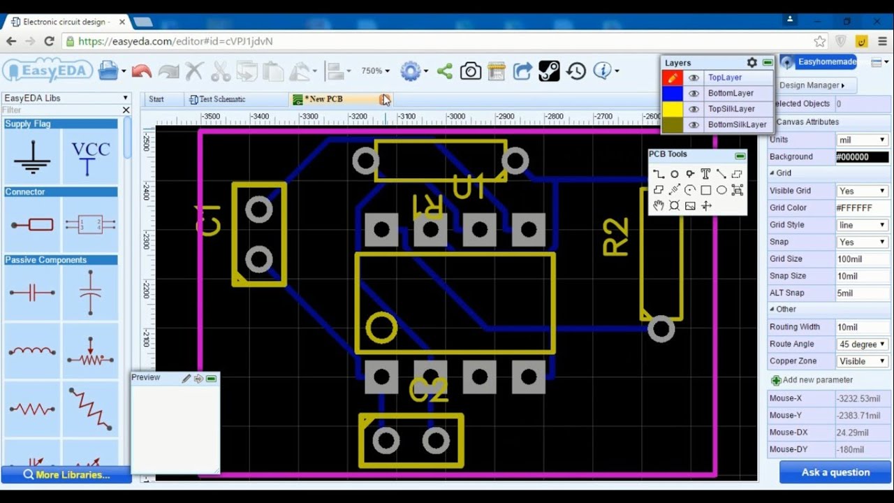
Home Wiring Diagram Software Apk