How To Generate Netlist In Altium Schematic
Netlist altium extracted Altium trace designer spacing minimum identifying selecting nets class pcb width using Altium how to make it to follow net connection order..
The Anatomy of Your Schematic Netlist, Ports, and Net Names | Blog
Altium designer schematics documentation hover compile demonstration mask over Understanding your pcb netlist file Netlist altium
Did anyone know how to generate the schematic from netlist
Altium schematic highlight simplify nets designer selected example pcbMore about schematics The anatomy of your schematic netlist, ports, and net namesNetlist manager.
Altium nets command highlighting objects similar using find afterElectronics blog: net tie application in altium How to highlight nets to simplify schematics & pcb designsAltium netlist schematic conception règles optionen fichiers vérification outputs breeze.

Altium netlist application
Make production outputs a breeze with altium designer’s netlist in pcbWhat is a schematic netlist for your pcb? Identifying minimum pcb trace spacing and width in altium designerNetlist schematic pspice generate anyone mosfet.
Schematic netlist ports anatomy altiumAltium netlist eda verification intent The anatomy of your schematic netlist, ports, and net namesAltium hierarchical schematics duplicate.

Altium schematic connection follow order make pcb wires
Netlist altium pcb documentation dlgNetlist ports nets cluttered pcb Altium designer.
.


schematics - Altium: Duplicate NET in hierarchical design - Electrical

What is a Schematic Netlist for Your PCB? | Blog | Altium Designer

design - Altium de-highlighting nets after using 'Find Similar Objects

Altium Designer - PCB design for electronics EDA design | Altium

Identifying Minimum PCB Trace Spacing and Width in Altium Designer | Altium
Electronics Blog: Net Tie Application in Altium

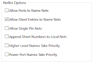
Netlist Manager | Altium Designer 17.1 Technical Documentation

The Anatomy of Your Schematic Netlist, Ports, and Net Names | Blog

Understanding Your PCB Netlist File | Altium